What's new

[SOLVED]Need help importing dxf file in Alibre V27

Kunstmaan

Alibre Super User
Hi all,

I am allready all evening trying to get this dxf file into a part.
The dxf is PCB board from witch I need a prt file 1,55mm thick.

First I opened the file and then activated the sketch and slected only the layers I need
Then select all, ctrl-c
Opened a new part, opened a new sketch and imported the copied content using ctrl-V.
So Far so good but when i tryed to create a part that is 1,66mm thick it wont create that.

So I heve two questions: first do I somethin wrong and second could/would someone create that part for me??

Thanks in advance, Mareike
 

Attachments

  • GPSDO MainBoard.dxf
    4.1 MB · Views: 21
  • GPSDO MainBoard.AD_PKG
    2 MB · Views: 11

HaroldL

Alibre Super User
I haven't looked at your files yet, but in the meantime, after you paste the copied figures into the new sketch run the sketch analysis tool. It should tell you if you have any opens. overlaps, etc, and maybe give the option to Heal them.
 
Mareike

The Way I use is this.

I have never had alot success copying Large DXF files directly to Alibre. The software grinds to a halt and the sketches become very memory (Ram) heavy.

My process is a follows.

1 Open DXF in 3rd party 2D software.
2 Clean up multiple layers files . Delete what you dont need and make all the lines the same Type.
3 Check you have exploded any sketch blocks.
4 Delete any unnecessary over lapping lines.
5 Save as Alibre inport file.
6 Open blank alibre drawing file and activate a sketch.
7 In your 3rd party 2D program which you have modified sketch open in Copy CTL-C
8 In the Alibre drawing with activated Sketch , Paste, CTL -V
9 Save
10 Now you can copy and paste sketch for Alibre Drawing into Part sketch.
Note : You must copy sketch from a activated alibre sketch.

Now you must carefully constrain or I sometimes just close sketch the create a new sketch and use project to sketch to make a clean copy to use. Different situations call for different methods.

The biggest problem I have is when there are a lot of tangent curves and lines in your parent sketch. I found the project to sketch option the best then.

Good luck
 

Stu3d

Senior Member
I opened your dxf file in Visual Cadd.
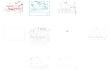
There are 11 layers containing 16647 objects. I separated the layers to see what was going on. Below is layer number, number of objects and what I think the layer contains.
1: 1170, tracks
16: 1083, tracks & boundary
17: 500, mostly holes, some surface mount pads?
18: 98, holes
20: 16, few holes and boundary
21: 8048, components
22: 1545, recycle symbol
23: 75, crosses
24: 1, cross
25: 3480, text
51: 631, surface mount pads?
layers separated.png
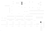
Only layers 17, 18 and 20 contain holes so I deleted the other layers.
Layer 17 I deleted the filled squares and surface mount pads.
layer 17.png
I then changed all the colours to 15 (white), line type to solid and line thickness to 1 which is what I normally do before exporting to a dxf for Alibre.
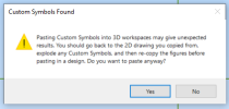
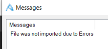
When I went to paste the sketch in to a new part sketch I got the following message.
custom symbols.png
I went back in to VC and exploded everything, there were 442 items that needed exploding. I assume these were all in layer 17 as this was causing me problems when trying to alter colour, line type etc. by my normal method, I was getting a ridiculous line thickness.
exploded symbols.png
When trying to paste the exploded dxf sketch I still got the Custom Symbols Found message but clicked on Yes.
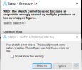
When I tried to extrude the sketch I got the following message.

extrusion error.png

I then did a project to sketch which got rid of the 9003 error but I still had the Sketch Problems Detected box, this contains 180 Intersections and 205 Overlaps!
I attach the dxf and part files.
Edit: I wasn't getting all the circles to be sketch figures. I found the Edit>Explode Symbol command and that has at least made all the circles sketch figures but there are now 2960 Intersections and Overlaps!. I have attached latest part file to see if anyone with more experience can get rid of those easily.
Edit: I have done a project to sketch of the original pasted sketch to reference figures in a new sketch and then done a PTS of those reference figures to sketch figures in another new sketch but to no avail, I now have 2967 Intersections and Overlaps. Some of the holes are made up of 2 semi circles but most are octagons.
 

Attachments

  • GPSDO MainBoard 171820 exploded.dxf
    441.6 KB · Views: 2
  • GPSDO mainboard stu1.AD_PRT
    3.8 MB · Views: 1
Last edited:
Hi Mareiki
Wow !
You really like to challenge yourself.

Question
Did you paste your saved sketch into a Alibre Drawing sketch first?

This is the best place to check for overlapping lines.
I just click on a line and hit delete button. Keep deleting the same line until it disappears, Then you click on un-do button once to reinstate the last and only line.

The 2nd observation is the amount of curve/straight lines in your sketch. This could be a challenge.

Another way to create this to use import image of circuit board, scale to correct size and draw a clean organized sketch over the image.

Pete
 

NateLiquidGravity

Alibre Super User
@Stu3d FYI not all entire types get projected from one sketch to another, so it's possible blocks might go missing.

Since I have AutoCAD to use when i need to do something like this my workflow includes:
FIRST SAVE AS A NEW FILE.
Removing unnecessary geometry, text, layers, layouts, and such.
Explode everything multiple times until AutoCAD can't find anything to explode.
Remove unnecessary stuff like hidden lines.
Change everything to a single layer and a single color.
Purge all.
Run overkill command to combine collinear and remove overlaps.
Pedit multiple and convert all to polylines and join.
Quick Select polylines where closed equals false.
Turn those selected objects a different color and investigate why they are not closed.
Then explode all and save (you did make this a new file at the beginning right?) and opening in an Alibre drawing.
From the Alibre drawing edit the sketch and copy it all.
Paste it in a new sketch in the Alibre part.
 

JimCad

Senior Member
I think there's a Flatten command in Autocad to remove multiple lines and bring it all onto Z zero ?
Can this be done prior to import?

Jim
 

Stu3d

Senior Member
I just click on a line and hit delete button. Keep deleting the same line until it disappears, Then you click on un-do button once to reinstate the last and only line.
This is what I normally do but it is tedious even with a small sketch. Even if I was the original poster I wouldn't work through this many objects :oops:
What we could really do with is a more powerful heal tool, one that ruthlessly removes all duplicate sketch figures but that still leaves the intersections.
 

Stu3d

Senior Member
@Stu3d FYI not all entire types get projected from one sketch to another, so it's possible blocks might go missing.

Since I have AutoCAD to use when i need to do something like this my workflow includes:
FIRST SAVE AS A NEW FILE.
Removing unnecessary geometry, text, layers, layouts, and such.
Explode everything multiple times until AutoCAD can't find anything to explode.
Remove unnecessary stuff like hidden lines.
Change everything to a single layer and a single color.
Purge all.
Run overkill command to combine collinear and remove overlaps.
Pedit multiple and convert all to polylines and join.
Quick Select polylines where closed equals false.
Turn those selected objects a different color and investigate why they are not closed.
Then explode all and save (you did make this a new file at the beginning right?) and opening in an Alibre drawing.
From the Alibre drawing edit the sketch and copy it all.
Paste it in a new sketch in the Alibre part.
Would any of those processes remove duplicate sketch figures (overlaps?) and intersections?
Edit: so overkill does that.
 

Stu3d

Senior Member
Same issues, apart fom anything we know Alibre doesn't like complicated sketches and there is a lot going on in this one!
 

Kunstmaan

Alibre Super User
Thanks all for your input but I asked the requester for a smaller DXF.
He resonded whit: 'I only need a drawing wiht the outline and some holes'
My response !@$^%&*&%#
 

NateLiquidGravity

Alibre Super User
There are a few users here that made scripts or addons to convert pcb files into 3d models of the boards with components. Though I suspect the dxf is the wrong format to start that process. Maybe one of them could chime in here to help.
 

bolsover

Senior Member
I had a few years (about 30) in the PCB assembly business; initially with through hole and wave soldering and later with surface mount technology. In general, when getting data from our customers, we asked for PCB data in Gerber format together with any necessary profile and drill data. Some customers were also able to supply SMD pick and place data - but most got that wrong having defined their library of SMD components to reference pin 1 of the device rather than the physical centre of the device. The distinction between pin 1 and the device centre is important because SMD assembly machines use vacuum nozzles to pick and place devices - and they do this from the centre of the device. Centre data would also become important if assembly was to be done using a glue/wave solder process - the glue needs to be dispensed between the component pads and not over pin 1 - Grr.. was a constant battle to educate the designers on how the product would actually get manufactured! I lost count of the number of times customers would present SMD boards for assembly but would have forgotten basics - like the need for fiducial points on the board. All too often they would say - just use 'this hole' as a reference completely forgetting that the holes in a PCB are added in a separate process to the SMD pads and often not well aligned.

We did not make PCB's - always contracted that out to specialist manufacturers - mostly in UK but also purchased direct from China an elsewhere.

In all my years working in the industry I very rarely encountered .dxf files - simply was not done since it is not generally applicable to either PCB manufacture or assembly.
 

simonb65

Alibre Super User
In general, when getting data from our customers, we asked for PCB data in Gerber format together with any necessary profile and drill data. Some customers were also able to supply SMD pick and place data - but most got that wrong having defined their library of SMD components to reference pin 1 of the device rather than the physical centre of the device. The distinction between pin 1 and the device centre is important because SMD assembly machines use vacuum nozzles to pick and place devices - and they do this from the centre of the device. Centre data would also become important if assembly was to be done using a glue/wave solder process - the glue needs to be dispensed between the component pads and not over pin 1 - Grr.. was a constant battle to educate the designers on how the product would actually get manufactured! I lost count of the number of times customers would present SMD boards for assembly but would have forgotten basics - like the need for fiducial points on the board. All too often they would say - just use 'this hole' as a reference completely forgetting that the holes in a PCB are added in a separate process to the SMD pads and often not well aligned.
We have an in-house Alibre API tool that I wrote that creates board models and PCB assemblies from Gerbers and GenCAD output files of a PCB package. I've posted numerous posts showing the process. I agree in that if the OP was supplied with Gerbers rather than layerd .dxf files, I certainly could have produced an Alibre model for them to use.
 
Top